CXR
CXR
Unlocking the Future of AI Hardware with CXR: Democratizing CMOS+X Innovation
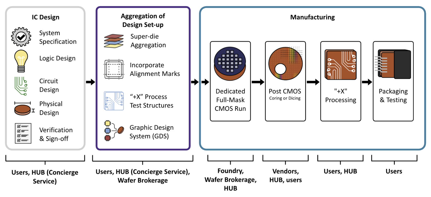
The integration of commercial-grade semiconductor CMOS technologies with emerging "X" technologies—such as 2D materials, quantum components, and functional materials—represents a transformative leap beyond traditional device scaling. This convergence not only overcomes the limitations of conventional semiconductor approaches but also accelerates the path to commercialization. However, innovators face significant barriers in accessing the necessary infrastructure: high design and mask costs for foundry runs, intellectual property (IP) concerns in multi-project wafer (MPW) services, and a lack of post-processing expertise for integrating "X" technologies. These challenges restrict the adoption of CMOS+X solutions to only a select few, stifling broader innovation.
To bridge this gap, the NW-AI Hub introduces CXR (CMOS +X Route), a pioneering initiative designed to democratize access to CMOS+X technologies for AI hardware implementation. By leveraging commercial-grade fabrication resources and specialized technical expertise, CXR empowers innovators, startups, and industry partners to rapidly prototype and scale next-generation semiconductor solutions.
CXR Journey
Why CMOS+X? A Faster Path from Research to Commercialization
Unlike approaches requiring fundamental CMOS-level retooling, CMOS+X builds on existing industry infrastructure, dramatically shortening the timeline from concept to market-ready technology. This makes it an attractive strategy for researchers, funding agencies, and commercial partners seeking near-term impact.
Key Benefits of CXR
- Streamlined Access to Advanced Fabrication
- Aggregates multiple research projects into cost-effective Multi-Project Wafer (MPW) runs, eliminating the prohibitive costs of standalone foundry access.
- Ensures IP protection and confidentiality, addressing a critical limitation of traditional commercial MPW services.
- End-to-End Post-Processing Expertise
- Provides seamless integration of "X" technologies through partnerships with leading facilities, including Berkeley Marvell Nanolab, Stanford Nanofabrication Facility (SNF), UC Davis Center for Nano-MicroManufacturing (CNM2), and Western Digital’s Nanoscale Lab.
- Enables rapid prototyping, testing, and optimization of hybrid CMOS+X devices.
Driving the Next Wave of AI Hardware Innovation
CXR removes the traditional barriers to CMOS+X adoption, fostering a collaborative ecosystem where researchers and industry can accelerate breakthroughs in AI, quantum computing, and beyond. By providing scalable, cost-efficient, and secure access to cutting-edge semiconductor technologies, CXR ensures that the next generation of hardware innovation is not limited to a few—but accessible to all.
Future Updates
For additional details and future updates regarding the next CXR shuttle, please visit our subpage below. A CXR Information Session for the second shuttle will be held on March 17, 2026.
For participation and partnership inquiries:
pacific-nw-ai-hub@stanford.edu
Join the CMOS+X advantage. Scale faster. Innovate without limits.