Workforce Development (WFD)
Mission Statement for WFD
California and Oregon employ over one third of the U.S. semiconductor workforce and Hawaii is a major center for defense technology. Our region is home to R&D facilities for leading chip manufacturers, equipment providers, chip design firms, and innovative startups, all of which drive a regional need for a pathway into the workforce. The Northwest-AI-Hub allocates 20% of its operating budget to workforce development, demonstrating a deep commitment to three objectives: (1) cultivate the local technician workforce through university fab internships for community college students and veterans, (2) democratize integrated circuits (IC) design education with new, open-source curricula, and (3) address the "exposure gap" through K-12 engagement. Our end goal is a vibrant workforce ecosystem that is greater than the sum of its parts.
Priority 1: Regional Technician Training
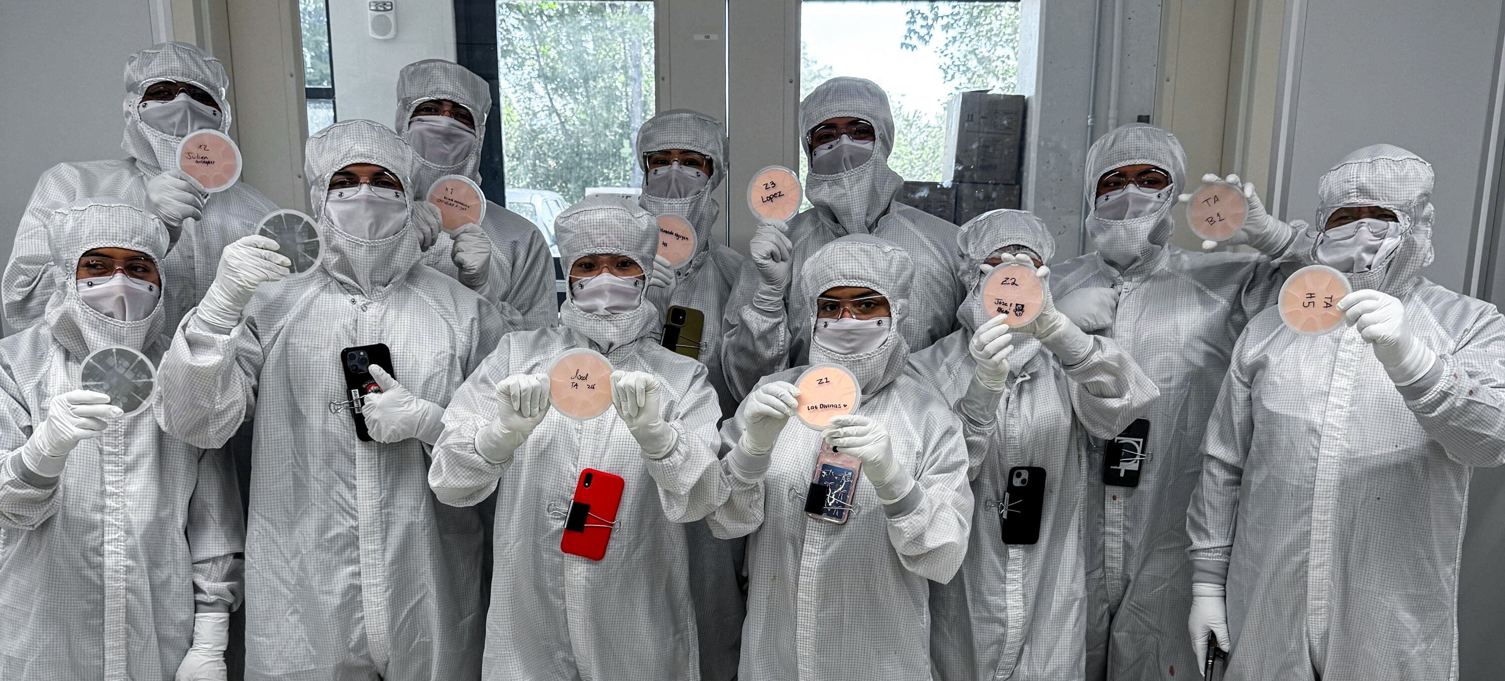
The semiconductor workforce is graying, with nearly 40% over age 50 and less than 25% under 35 (SIA report May 2021). 44% of employees do not have bachelor’s degrees, a demographic with the least geographic mobility. For this reason, we will partner with regional community colleges to cultivate a pathway into a local technician workforce through hands-on, paid internships and professional development programs. Hub funding will enable each university to expand on its own, local internship program and coordinate professional development opportunities across the Hub. We aim to build a supportive and collaborative community that leverages our collective resources to expand the number of candidates and the ways they can enter the semiconductor workforce. We will build on existing fab internship programs and create pathways for interns to pursue further internship and professional opportunities with Hub partners.
Priority 2: Open-Source Chip Design Course
The industry has a need for IC design professionals who are fluent in electronic design automation (EDA) and process design kits (PDKs), but current teaching toolkits to train them are lacking. The Northwest-AI-Hub will establish and maintain a platform for exchange of open-source laboratory exercises and design flows using open-source platforms to enable complete design of systems‐on‐a‐chip (SoC). We will develop chip design flows as well as repositories of complex IP blocks to enable curriculum development through community supported shared expertise. The Hub will cultivate the chip design community through design contests that make use of open-source technologies and cloud environments for lowering the barrier-to entry and increasing participation and awareness of chip design, as well as meetups at major conferences where community members share best practices for design and course building, and students can network with industry professionals to seek internships and full-time jobs.
Priority 3: K-12 Engagement and Beyond
Building a pathway into the professional workforce starts by exposing students to exciting opportunities in STEM. Every year, the Hub supports a Stanford-hosted teacher professional development workshop, Nanoscience Summer Institute for Middle School Teachers (NanoSIMST), which provides educators with a paid, hands-on learning experience. Participants are introduced to cutting-edge technology and nanoscience concepts that can be brought into the classroom to engage students with real-world challenges. Teachers receive instructional materials, guidance, access to guest speakers, exposure to high-demand career paths, and a wealth of online resources.
Through programs like this and many others, the Hub will enhance existing, successful programs by connecting people and resources, leveraging opportunities through a shared commitment to inspire more students to explore and succeed in STEM.

